


With the circuit technology entering the era of ultra-large-scale integration, the high complexity of the circuit and the application of multi-layer printed board, surface mount and multi-chip module technology in the circuit system make the physical accessibility of many circuit nodes gradually weaken or even disappear, the testability of the circuit and system drops sharply, and the proportion of test overhead in the total cost of the circuit and system keeps rising. The traditional test scheme of AOI+ICT can no longer meet the test and fault diagnosis of existing products.
Especially in the server market, with the increasing output requirements and stricter quality requirements, product testing is facing great challenges with the increasing complexity of products. At present, almost all complex chips have integrated JTAG control interface (TCK/TMS/TDI/TDO/TRST), and JTAG control logic is simple, convenient and easy to implement.

Boundary scan testing is a software-based testing solution with very little hardware intervention.
Its advantages include:
1.It is convenient to locate the fault of the chip, quickly and accurately test whether the connection of two chip pins is reliable, and improve the testing efficiency;
2.The chip with JTAG interface has some predefined functional modes built in, and the chip is in a specific functional mode through boundary scanning channel, so as to improve the flexibility of system control and facilitate system design;
3. It is suitable for R&D and laboratories to detect faults in product design stage in advance;
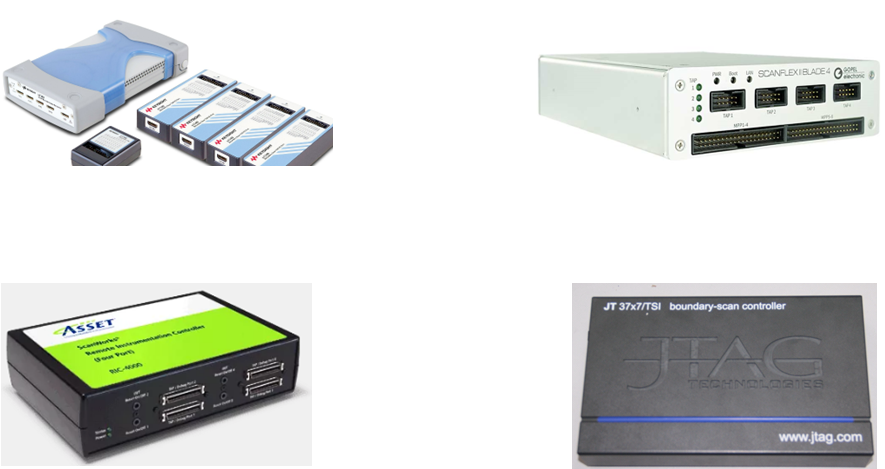
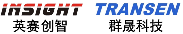
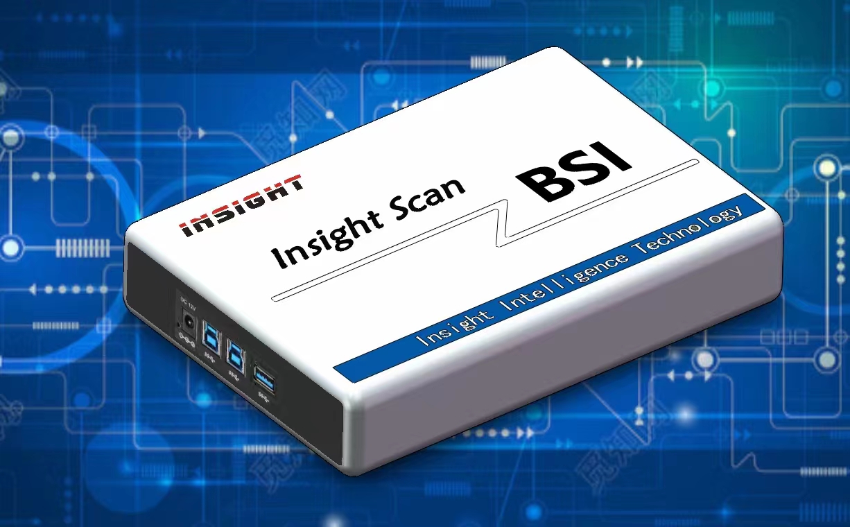
4. It is suitable for mass production, improving the coverage of product testing and ensuring the quality of products.At present, most electronic product tests use the following boundary scan controllers: